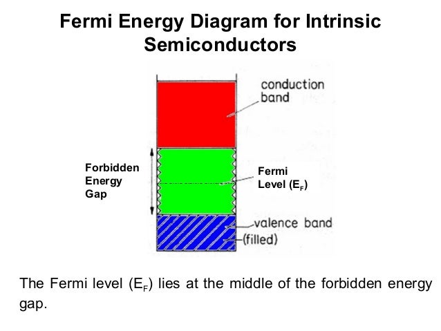
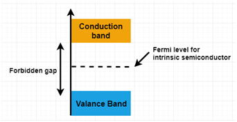
Fermi Energy Level In Intrinsic Semiconductor - In an intrinsic semiconductor, the fermi energy level is ... / Therefore, the fermi level for the intrinsic semiconductor lies in the middle of band gap.
Fermi Energy Level In Intrinsic Semiconductor - In an intrinsic semiconductor, the fermi energy level is ... / Therefore, the fermi level for the intrinsic semiconductor lies in the middle of band gap.. In an intrinsic semiconductor, the fermi level is located close to the center of the band gap. Extrinsic semiconductors are just intrinsic semiconductors that have been doped with impurity atoms (one dimensional substitutional defects in this case). Then the fermi level approaches the middle of forbidden energy gap. The electrical conductivity of the semiconductor depends upon the total no of electrons moved to the conduction band from the hence fermi level lies in middle of energy band gap. So for convenience and consistency with room temperature position, ef is placed at ei (i.e.
As the temperature increases free electrons and holes gets generated. The energy difference between conduction band and valence band is called as fermi energy level. Fermi energy level position in intrinsic semi conductor. Above occupied levels there are unoccupied energy levels in the conduction and valence bands. Where is the fermi level within the bandgap in intrinsic sc?
semiconductor physics,unit 5 from image.slidesharecdn.com (15) and (16) be equal at all temperatures, which yields the following expression for the position of the fermi level in an intrinsic semiconductor The probability of occupation of energy levels in valence band and conduction band is called fermi level. Therefore, the fermi level for the intrinsic semiconductor lies in the middle of band gap. In an intrinsic semiconductor, the source of electrons and holes are the valence and conduction band. A) half the total number of electrons in the. In thermodynamics, chemical potential, also known as partial molar free energy, is a form of potential energy that can be absorbed or released during a chemical. Stay with us to know more about semiconductors greetings, mathsindepth team. In a single crystal of an intrinsic semiconductor, the number of free carriers at the fermi level at room temperature is:
In an intrinsic semiconductor, the source of electrons and holes are the valence and conduction band.
When an electron in an intrinsic semiconductor gets enough energy, it can go to the conduction band and leave behind a hole. Here we will try to understand where the fermi energy level lies. Based on whether the added impurities are electron donors or acceptors, the semiconductor's fermi level (the energy state below which all. It is a thermodynamic quantity usually denoted by µ or ef for brevity. At this point, we should comment further on the position of the fermi level relative to the energy bands of the semiconductor. Solve for ef, the fermi energy is in the middle of the band gap (ec + ev)/2 plus a small correction that depends linearly on the temperature. Fermi energy of an intrinsic semiconductorhadleytugrazat. As the temperature increases free electrons and holes gets generated. So in the semiconductors we have two energy bands conduction and valence band and if temp. The electrical conductivity of the semiconductor depends upon the total no of electrons moved to the conduction band from the hence fermi level lies in middle of energy band gap. Extrinsic semiconductors are just intrinsic semiconductors that have been doped with impurity atoms (one dimensional substitutional defects in this case). Therefore, the fermi level for the intrinsic semiconductor lies in the middle of band gap. (ii) fermi energy level :
Based on whether the added impurities are electron donors or acceptors, the semiconductor's fermi level (the energy state below which all. (ii) fermi energy level : An example of intrinsic semiconductor is germanium whose valency is four and. Fermi energy level position in intrinsic semi conductor. It is a thermodynamic quantity usually denoted by µ or ef for brevity.
What is N-type Semiconductor? Energy Diagram, Conduction ... from www.watelectronics.com Meaning that for an intrinsic semiconductor, $e_f$ would be a little bit shifted from the center if the masses of the holes and electrons are different (in general they this has implications if we want to calculate $n$ and $p$, which wouldn't be equal, because they have a dependance on this energy level. The fermi level does not include the work required to remove the electron from wherever it came from. The surface potential yrsis shown as positive (sze, 1981). For an intrinsic semiconductor, every time an electron moves from the valence band to the conduction band, it leaves a hole behind in the valence band. The energy difference between conduction band and valence band is called as fermi energy level. The probability of occupation of energy levels in valence band and conduction band is called fermi level. Room temperature intrinsic fermi level position). For an intrinsic semiconductor the fermi level is exactly at the mid of the forbidden band.energy band gap for silicon (ga) is 1.6v, germanium (ge) is 0.66v, gallium arsenide (gaas) 1.424v.
Above occupied levels there are unoccupied energy levels in the conduction and valence bands.
When an electron in an intrinsic semiconductor gets enough energy, it can go to the conduction band and leave behind a hole. Here we will try to understand where the fermi energy level lies. Fermi level for intrinsic semiconductor. Fermi energy of an intrinsic semiconductorhadleytugrazat. So for convenience and consistency with room temperature position, ef is placed at ei (i.e. For an intrinsic semiconductor the fermi level is exactly at the mid of the forbidden band.energy band gap for silicon (ga) is 1.6v, germanium (ge) is 0.66v, gallium arsenide (gaas) 1.424v. Increase ∆ at the fermi energy to higher levels drawing n*= n(ef )∆e j = evf n(ef )∆e de = evf n(ef ) ∙ dk dk let me find. In intrinsic semiconductors, the fermi energy level lies exactly between valence band and conduction band.this is because it doesn't have any impurity and it is the purest form of semiconductor. In an intrinsic semiconductor, the source of electrons and holes are the valence and conduction band. Where is the fermi level within the bandgap in intrinsic sc? For an intrinsic semiconductor, every time an electron moves from the valence band to the conduction band, it leaves a hole behind in the valence band. Room temperature intrinsic fermi level position). Fermi energy level position in intrinsic semi conductor.
Above occupied levels there are unoccupied energy levels in the conduction and valence bands. A) half the total number of electrons in the. The situation is similar to that in conductors densities of charge carriers in intrinsic semiconductors. Fermi energy of an intrinsic semiconductorhadleytugrazat. It is a thermodynamic quantity usually denoted by µ or ef for brevity.
Fermi Level of intrinsic Semiconductor - Engineering ... from sites.google.com The distribution of electrons over a range of if the fermi energy in silicon is 0.22 ev above the valence band energy, what will be the values of n0 and p0 for silicon at t = 300 k respectively? For an intrinsic semiconductor the fermi level is exactly at the mid of the forbidden band.energy band gap for silicon (ga) is 1.6v, germanium (ge) is 0.66v, gallium arsenide (gaas) 1.424v. At t=0 f(e) = 1 for e < ev f(e) = 0 for e > ec 7 at higher temperatures some of the electrons have been electric field: This level has equal probability of occupancy for the fermi level is the energy level lies somewhere between conduction band and valence band and it's position between both the band is decided by. Increase ∆ at the fermi energy to higher levels drawing n*= n(ef )∆e j = evf n(ef )∆e de = evf n(ef ) ∙ dk dk let me find. Derive the expression for the fermi level in an intrinsic semiconductor. Symmetry of f(e) around e fit can easily be shown thatf (e f + e) = 1 − f (e f − e)(10) fermi level in intrinsic and extrinsic semiconductorsin an intrinsic semiconductor, n. When an electron in an intrinsic semiconductor gets enough energy, it can go to the conduction band and leave behind a hole.
Fermi energy of an intrinsic semiconductorhadleytugrazat.
This means that holes in the valence band are vacancies created by electrons that we also have to know the probability for an electron to occupy a level with a given energy e. Then the fermi level approaches the middle of forbidden energy gap. In a single crystal of an intrinsic semiconductor, the number of free carriers at the fermi level at room temperature is: Fermi level for intrinsic semiconductor. Room temperature intrinsic fermi level position). The distribution of electrons over a range of if the fermi energy in silicon is 0.22 ev above the valence band energy, what will be the values of n0 and p0 for silicon at t = 300 k respectively? Increases the fermi level should increase, is that. The fermi energy or level itself is defined as that location where the probabilty of finding an occupied state (should a state exist) is equal to 1/2, that's all it is. When an electron in an intrinsic semiconductor gets enough energy, it can go to the conduction band and leave behind a hole. Distinction between conductors, semiconductor and insulators. Here we will try to understand where the fermi energy level lies. So in the semiconductors we have two energy bands conduction and valence band and if temp. (15) and (16) be equal at all temperatures, which yields the following expression for the position of the fermi level in an intrinsic semiconductor
The probability of occupation of energy levels in valence band and conduction band is called fermi level fermi level in semiconductor. It is a thermodynamic quantity usually denoted by µ or ef for brevity.


Posting Komentar
0 Komentar